
How long does it take for PCB immersion gold?
The surface treatment process of PCB board includes: anti-oxidation, HASL, lead-free HASL, immersion gold, immersion tin, immersion silver, hard gold plating, full board gold plating, gold finger, nickel palladium gold OSP, etc. The main requirements are: low cost, good weldability, harsh storage conditions, short time, environmental protection process, good welding and smoothness. The immersion gold adopts the method of chemical deposition, which forms a layer of coating through the method of chemical oxidation-reduction reaction, which is generally thicker. It is a kind of deposition method of chemical nickel-gold-gold layer, which can achieve a thicker gold layer.
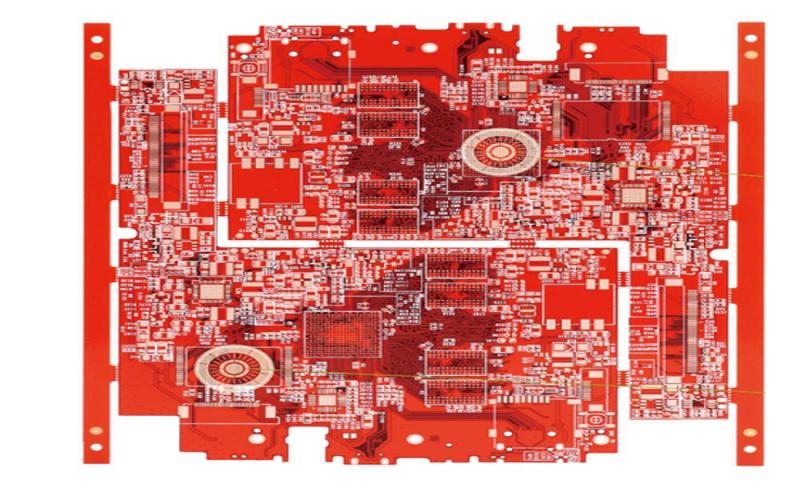
What are the advantages of PCB immersion gold? The advantage of the immersion gold process is that the deposited color on the surface is very stable when the circuit is printed, the brightness is very good, the coating is very smooth, and the solderability is very good. Immersion gold generally has a thickness of 1-3 Uinch, so the surface treatment method of immersion gold is generally thicker, so the surface treatment method of immersion gold is widely used in key boards, gold finger boards and other circuit boards. Because gold has strong conductivity, good oxidation resistance and long service life.
How long does it take for PCB immersion gold to be baked?
(1) If it is sealed and unsealed for more than 5 days within 2 months from the date of manufacture, bake at 120±5°C for 1 hour.
(2) 2 months after the date of manufacture, bake at 120±5°C for 1 hour before going online.
(3) 2 to 6 months after the date of manufacture, bake at 120±5°C for 2 hours before going online.
(4) 6 to 12 months after the date of manufacture, bake at 120±5°C for 4 hours before going online.
(5) The baked PCB must be used within 5 days (put into IR REFLOW), and the unused PCB needs to be baked for another 1 hour before it can be used online.
(6) One year after the date of manufacture, bake at 120±5°C for 4 hours before going online, and then send it to the PCB factory for re-spraying tin before going online.
What are the PCB baking methods?
(1) Large PCBs (16 PORTs or more including 16 PORTs) are placed flat, with a maximum of 30 pieces in a stack. Open the oven within 10 minutes after baking, take out the PCB and place it flat to cool naturally (press-proof board bay fixtures are required)
(2) Small and medium-sized PCBs (including 8 PORTs below 8 PORTs) are placed flat, with a maximum of 40 pieces in a stack, and there is no limit to the number of vertical ones. Open the oven within 10 minutes after baking and take out the PCB. Banwan fixture)
Send PCB Files to Sales@ucreatepcba.com, We Will Quote You Very Soon!
Request PCB Manufacturing & Assemble Quote Now


