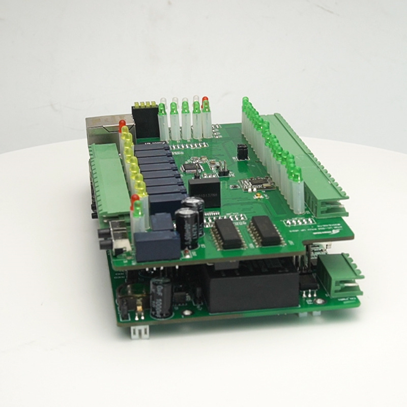
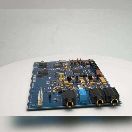
Ucreate Medical Rigid PCB / Multilayer Printed Board
|
Layer: |
6 Layer |
|
Material: |
IT180A |
|
PCB Thickness: |
0.8mm |
|
Cu Thickness: |
1.5 OZ |
|
Min Line W/S: |
0.1/0.1mm |
|
Surface Finish: |
Immersion gold |
|
Certificate: |
UL/ISO/TS16949/RoHS/IATF |
|
Application: |
Medical Electronics |
We will reply within 2 hours!
Product Parameters
Item | Specifica |
Layers | 1~32 |
Board thickness | 0.1mm-7.0mm |
Material | FR-4,CEM-1/CEM-3,PI,High Tg,Rogers |
Max panel size | 32"×48"(800mm×1200mm) |
Min hole size | 0.075mm |
Min line width | 3mil(0.075mm) |
Surface finish | OSP,HASL,Imm Gold/Nickel/Ag, Electric gold |
Copper thickness | 0.5-7.0OZ |
Soldermask | Green/Yellow/Black/White/Red/Blue |
Silkscreen | Red/Yellow/Black/White |
Min PAD | 5mil(0.13mm) |
Inter package | Vacuum |
Outer package | Carton |
Outline tolerance | ±0.75mm |
Hole tolerance | PTH:±0.05 NPTH:±0.025 |
Certificate | UL,ISO 9001,ISO14001,IATF16949 |
Special request | Blind hole+Gold finger + BGA |
Material Suppilers | Shengyi, KB, Nanya, ITEQ,etc. |
General Introduction of Multilayer PCB
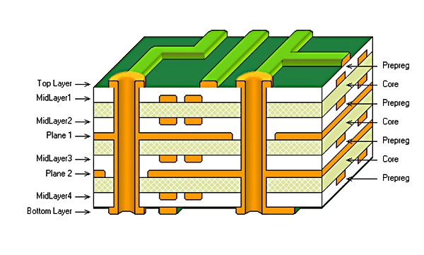
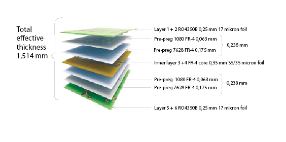
As the name suggests, a multi-layer circuit board can only be called a multi-layer circuit board with more than two layers, such as four layers, six layers, eight layers, and so on. Of course, some designs are three-layer or five-layer circuit, also called multi-layer PCB circuit board.
Conductive wiring diagram larger than the two-layer board. The insulating substrate is separated between the layers. After each layer of the circuit is printed, each layer of the circuit is overlapped by pressing. After drilling, the electrical connection between them is usually achieved through plated through holes on the cross section of the circuit board.

One-stop Service Include
PCB Prototype | Quick Turn PCB | Single-Sided PCB |
Double-Sided PCB | Multilayer PCB | Rigid PCB |
Flexible PCB | Rigid-Flex PCB | LED PCB |
Aluminum PCB | Metal Core PCB | Thick Copper PCB |
HDI PCB | BGA PCB | High TG PCB |
PCB Stencil | Impedance Control PCB | PCB Assembly |
High-Frequency PCB | Bluetooth Circuit Board | Automotive PCB |
USB Circuit Board | Halogen-Free PCB | Antenna PCB |

