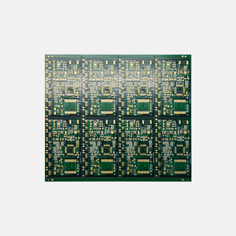
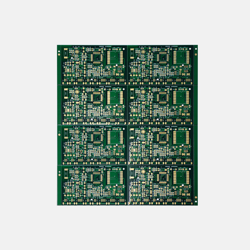
Definition of various layers in PCB circuit board design
PCB circuit board is an indispensable part of electronic products, and the definition of various layers in PCB circuit board design is an important link in the process of PCB circuit board manufacturing. When designing a PCB circuit board, it is necessary to understand the definitions of various layers to ensure the normal operation of the circuit board. This article will introduce the definition of various layers in PCB circuit board design.
1. Signal layer
The signal layer is one of the most important layers in PCB circuit board design and is used to transmit signals in the circuit. On the signal layer, the designer needs to draw the signal lines in the circuit diagram to ensure the normal operation of the circuit board. The signal layer is usually divided into the top signal layer and the bottom signal layer, which are located on the top and bottom of the board respectively.
2. Power layer
The power layer is the layer used to transmit power signals in PCB circuit board design. On the power layer, the designer needs to draw the power lines in the circuit diagram to ensure the normal operation of the circuit board. The power layer is usually divided into a positive power layer and a negative power layer, which are used to transmit positive power and negative power signals respectively.
3. Formation
The ground layer is the layer used to transmit the ground signal in the PCB circuit board design. On the ground layer, the designer needs to draw the ground line in the circuit diagram to ensure the normal operation of the circuit board. Strata are usually divided into top and bottom strata, which are located on the top and bottom of the board, respectively.
4. Pad layer
The pad layer is the layer used for soldering components in PCB circuit board design. On the pad layer, the designer needs to draw the pads of the components in order to solder the components. The pad layer is usually divided into a top pad layer and a bottom pad layer, which are located on the top and bottom of the board, respectively.
5. Silk screen layer
The silk screen layer is a layer used to mark circuit board information in PCB circuit board design. On the silk screen layer, designers can draw the name, version number, manufacturer information, etc. of the circuit board to facilitate the identification and maintenance of the circuit board. The silk screen layer is usually divided into a top silk screen layer and a bottom silk screen layer, which are located on the top and bottom of the circuit board respectively.
In short, the definition of various layers in PCB circuit board design is an important link in the PCB circuit board manufacturing process. When designing a PCB circuit board, it is necessary to understand the definitions of various layers to ensure the normal operation of the circuit board.


Send PCB Files to Sales@ucreatepcba.com, We Will Quote You Very Soon!
Request PCB Manufacturing & Assemble Quote Now


