Double-Sided / Multilayer Gold Finger PCB Fabrication
|
Layer: |
2 Layer |
|
Material: |
Fr-4 |
|
PCB Thickness: |
1.3mm |
|
Cu Thickness: |
1.0 OZ |
|
Min Line W/S: |
0.1/0.1mm |
|
Surface Finish: |
Immersion gold |
|
Certificate: |
UL/ISO/TS16949/RoHS/IATF |
|
Application: |
Computer Electronics |
We will reply within 2 hours!
Product Parameters
Item | Specifica |
Layers | 1~32 |
Board thickness | 0.1mm-7.0mm |
Material | FR-4,CEM-1/CEM-3,PI,High Tg,Rogers |
Max panel size | 32"×48"(800mm×1200mm) |
Min hole size | 0.075mm |
Min line width | 3mil(0.075mm) |
Surface finish | OSP,HASL,Imm Gold/Nickel/Ag, Electric gold |
Copper thickness | 0.5-7.0OZ |
Soldermask | Green/Yellow/Black/White/Red/Blue |
Silkscreen | Red/Yellow/Black/White |
Min PAD | 5mil(0.13mm) |
Inter package | Vacuum |
Outer package | Carton |
Outline tolerance | ±0.75mm |
Hole tolerance | PTH:±0.05 NPTH:±0.025 |
Certificate | UL,ISO 9001,ISO14001,IATF16949 |
Special request | Blind hole+Gold finger + BGA |
Material Suppilers | Shengyi, KB, Nanya, ITEQ,etc. |
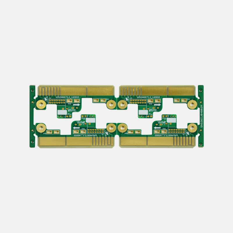
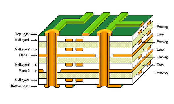
General Introduction of Multilayer PCB
As the name suggests, a multi-layer circuit board can only be called a multi-layer circuit board with more than two layers, such as four layers, six layers, eight layers, and so on. Of course, some designs are three-layer or five-layer circuit, also called multi-layer PCB circuit board.
Conductive wiring diagram larger than the two-layer board. The insulating substrate is separated between the layers. After each layer of the circuit is printed, each layer of the circuit is overlapped by pressing. After drilling, the electrical connection between them is usually achieved through plated through holes on the cross section of the circuit board.

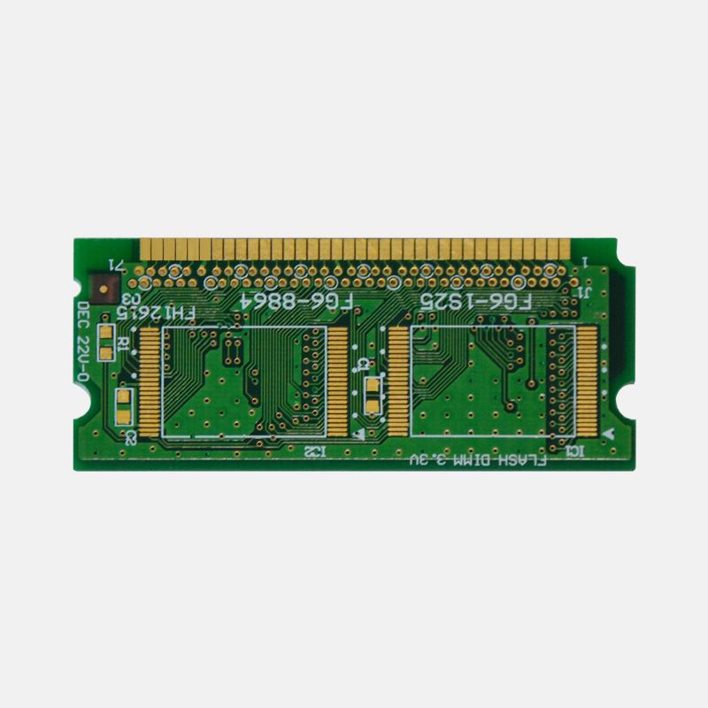
Gold Finger PCB
A Gold Finger PCB (Printed Circuit Board) is a type of circuit board that has gold-plated contact pads or fingers along its edges. These gold-plated pads are used for connecting the PCB to other electronic devices or components, typically using edge connectors or card-edge connectors.
Gold finger PCBs are commonly used in high-reliability applications where a secure and durable electrical connection is essential. The gold plating provides several benefits over other materials, including corrosion resistance, excellent conductivity, and good wear resistance. Gold is also an excellent material for soldering, which makes it ideal for applications where the PCB will be subjected to frequent or heavy use.
Request Gold Finger PCB & Assemble Quote Now
PCB Manufacturing Services
As one of the leading Printed Circuit Board manufacturers based in China, Ucreate has been offering international companies of all sizes with high-quality PCB prototype to production services at a fair price for eight years. To make professional and advanced circuit boards, we're committed to adhering to the strictest standards during the PCB manufacturing process. We're fully compliant with the ISO 9001:2008 quality management system.
One-stop Service Include
PCB Prototype | Quick Turn PCB | Single-Sided PCB |
Double-Sided PCB | Multilayer PCB | Rigid PCB |
Flexible PCB | Rigid-Flex PCB | LED PCB |
Aluminum PCB | Metal Core PCB | Thick Copper PCB |
HDI PCB | BGA PCB | High TG PCB |
PCB Stencil | Impedance Control PCB | PCB Assembly |
High-Frequency PCB | Bluetooth Circuit Board | Automotive PCB |
USB Circuit Board | Halogen-Free PCB | Antenna PCB |