
What are the commonly used laminated structures of HDI PCB boards?
High-Density Interconnect (HDI) printed circuit boards (PCBs) are increasingly popular in modern electronics due to their compact size, high functionality, and superior signal performance. HDI PCBs are known for their complex and intricate circuitry, which allows for more advanced electronic devices. One of the critical aspects of HDI PCB design is the choice of laminated structures. In this article, we will explore the commonly used laminated structures of HDI PCB boards and their significance in enhancing the overall performance and reliability of electronic devices.
1. Basic Structure of HDI PCBs
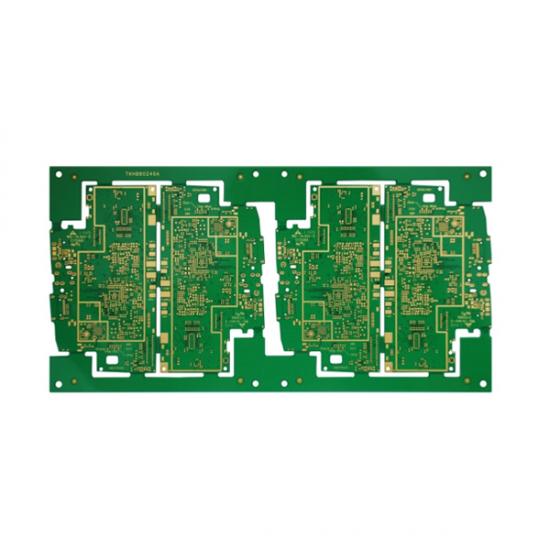
Before diving into the specific laminated structures, let's understand the basic construction of an HDI PCB. HDI PCBs are characterized by their higher wiring density, achieved through the use of microvias and high-density connections. These boards typically consist of several layers of copper traces and insulating materials sandwiched together.
2. Commonly Used Laminated Structures
a) 1+N+1 Structure: The 1+N+1 structure is one of the simplest and commonly used laminated structures in HDI PCBs. It consists of a single signal layer sandwiched between two layers of insulation, with microvias connecting the signal layer to the outer layers. This structure is suitable for designs with a moderate level of complexity and is cost-effective.
b) 2+N+2 Structure: The 2+N+2 structure is a step up from the 1+N+1 structure, featuring two signal layers between three insulation layers. The use of additional signal layers allows for increased routing capability and the ability to accommodate more complex designs with higher-density components.
c) 3+N+3 Structure: The 3+N+3 structure is a further advancement, providing three signal layers between four insulation layers. This laminated structure offers even greater routing density and design flexibility, making it suitable for highly complex and advanced electronic devices.
d) 4+N+4 Structure: The 4+N+4 structure is the most sophisticated and complex laminated structure commonly used in HDI PCBs. With four signal layers sandwiched between five insulation layers, this structure provides the highest level of routing capability and accommodates intricate designs with the most densely packed components.
3. Benefits of Different Laminated Structures
a) Improved Signal Integrity: Higher-density laminated structures, such as 3+N+3 and 4+N+4, offer enhanced signal integrity. The reduced length of signal traces and optimized routing reduce signal loss and crosstalk, resulting in improved overall signal performance.
b) Increased Design Flexibility: The use of more signal layers in laminated structures allows for greater design flexibility. Designers can route signals more efficiently, reduce the number of vias, and minimize signal distortion, leading to more reliable and efficient PCB layouts.
c) Miniaturization and Space Savings: HDI PCBs are known for their compact size and high component density. The advanced laminated structures enable the miniaturization of electronic devices and contribute to the reduction of overall PCB size, which is crucial in modern portable electronics.
d) Enhanced Thermal Management: Laminated structures with more insulation layers provide better thermal management for electronic components. The increased isolation between signal layers allows for efficient heat dissipation, preventing overheating and ensuring long-term reliability.
4. Considerations for Selecting Laminated Structures
The choice of laminated structure in HDI PCB design depends on various factors, including the complexity of the circuit, the number of components, signal integrity requirements, and available space. Designers must carefully evaluate these considerations to determine the most suitable laminated structure that meets the specific requirements of the electronic device.
Conclusion:
In conclusion, the laminated structure is a crucial aspect of High-Density Interconnect (HDI) PCB design, directly influencing the performance, reliability, and compactness of modern electronic devices. The commonly used laminated structures, such as the 1+N+1, 2+N+2, 3+N+3, and 4+N+4, offer different levels of design flexibility, signal integrity, and space savings. The selection of the appropriate laminated structure depends on the complexity of the circuit and the desired performance goals. As electronic devices continue to evolve and become more compact and powerful, the optimization of laminated structures in HDI PCB design will play an increasingly significant role in meeting the demands of the ever-changing technological landscape.
Send PCB Files to Sales@ucreatepcba.com, We Will Quote You Very Soon!
Request PCB Manufacturing & Assemble Quote Now


