
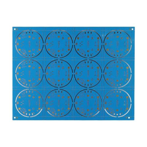
Single and Double-sided PCB Circuit Boards
PCB circuit boards can be divided into single-panel, double-panel and multi-panel. We usually use single-panel and double-panel, so what is the difference between single-panel and double-panel? Single-sided boards refer to single-sided circuit boards, with components on one side and wires on the other side; double-sided boards can lay out components and wiring on both sides. Because the single-sided panel has only one side and cannot be crossed, the wiring is more difficult, while the double-sided panel can be wired on both sides, and the wiring difficulty is low, which is more suitable for use in complex circuits. The production process of the double-sided board is more difficult than that of the single-sided board, mainly because the top and bottom layers of the copper clad laminate must be connected through holes and wired.
The difference between single-panel and double-panel is reflected in the following points:
1. In terms of technology: the welding of single-sided panels is concentrated on one side, and components are placed on the other side; both sides of double-sided panels can be welded, and both surface mount components and connectors can be placed.
2. In terms of material: single-sided panels have copper foil on only one side, while double-sided panels have copper foil traces on both sides, and the copper foils on both sides are connected through vias.
3. On the production process:
1) Production process of single panel:
Cutting→Drilling and positioning→Silk printing circuit→Etching→Silk printing text, curing→Mold punching shape→Circuit inspection and testing→Packaging and delivery
2) Production process of double panel:
Cutting → Drilling → Immersion Copper → Graphic Transfer → Graphic Plating → Etching → Stripping and Cleaning → Solder Mask → Silk Screen → Die Die Cutting Shape → Inspection and Testing → Packaging and Shipping
Although there are some differences between single-sided boards and double-sided boards, their structures are the same, including pads, vias, mounting holes, connectors, electronic components, wires, filling and electrical boundaries.
The working level is also the same, whether it is single-sided or double-sided, there are many types of working levels, such as signal layer, silk screen layer, solder mask layer, solder paste layer, ground layer, etc. Usually the circuit board has dozens of signal layers, which are used to place components related to the signal. The top layer is used to place components, the bottom layer is covered with copper, and the middle layer is used to place signal traces; the silk screen layer is used to draw the appearance of components and print product numbers. , component model, company name, etc.; the solder mask layer is to prevent the flow of solder, prevent solder from being stained with solder in places that do not need to be soldered, and cause short circuits in other components; the solder paste layer is used to paste SMD components on the circuit board, which is convenient Soldering; the ground plane is to connect the copper film of the ground plane to the ground pin.
The circuit board has developed from single-sided to double-sided and multi-sided, and is constantly developing in the direction of small size, high precision, high density, high reliability and high-speed transmission, which reduces production costs and improves product performance. Whether it is single-sided or double-sided, it maintains With a good development trend, it maintains a strong momentum in the development of electronic equipment.
Send PCB Files to Sales@ucreatepcba.com, We Will Quote You Very Soon!
Request PCB Manufacturing & Assemble Quote Now


