
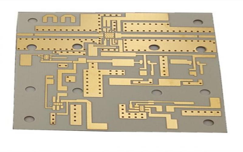
Why do PCB boards need plug holes?
The development of the electronics industry promotes the development of PCB circuit boards, and also puts forward higher requirements for printed board manufacturing technology and surface mount technology. The plug hole process came into being. PCB circuit board plug holes are usually placed after the solder mask layer, and then the second layer of ink is applied to fill the heat dissipation holes with a diameter of less than 0.55mm.
Why do PCB boards need plug holes?
Conductive hole Via hole is also known as conduction hole. In order to meet customer requirements, the circuit board via hole must be plugged. After a lot of practice, the traditional aluminum sheet plugging process is changed, and the circuit board surface is completed with white mesh. hole, stable production and reliable quality.
Via holes play the role of interconnection and conduction between lines. The development of the electronics industry also promotes the development of PCB, and also puts forward higher requirements for PCB manufacturing technology and SMT processing technology. The Via hole plugging process came into being, and the following requirements should be met at the same time:
1. There is only enough copper in the via hole, and the solder mask can be plugged or not;
2. There must be tin-lead in the via hole, with a certain thickness requirement (4 microns), and there must be no solder resist ink entering the hole, causing tin beads to be hidden in the hole;
3. The via holes must have solder resist ink plug holes, are opaque, and must not have tin circles, tin beads, and flatness.
With the development of electronic products in the direction of "light, thin, short and small", PCBs are also developing towards high density and high difficulty, so there are a large number of SMT and BGA PCBs, and customers require plug holes when mounting components. Five functions:
1. Prevent short circuit caused by tin penetrating through the component surface through the via hole during PCB wave soldering; especially when we put the via hole on the BGA pad, we must first make a plug hole and then gold-plate it to facilitate BGA soldering.
2. Avoid flux residues in via holes;
3. After the SMT processing and component assembly in the electronics factory are completed, the PCB needs to be vacuumed on the testing machine to form a negative pressure before it is completed:
4. Prevent the solder paste on the surface from flowing into the hole to cause false soldering and affect the placement;
5. Prevent tin balls from popping out during wave soldering, causing short circuits.
Send PCB Files to Sales@ucreatepcba.com, We Will Quote You Very Soon!
Request PCB Manufacturing & Assemble Quote Now


