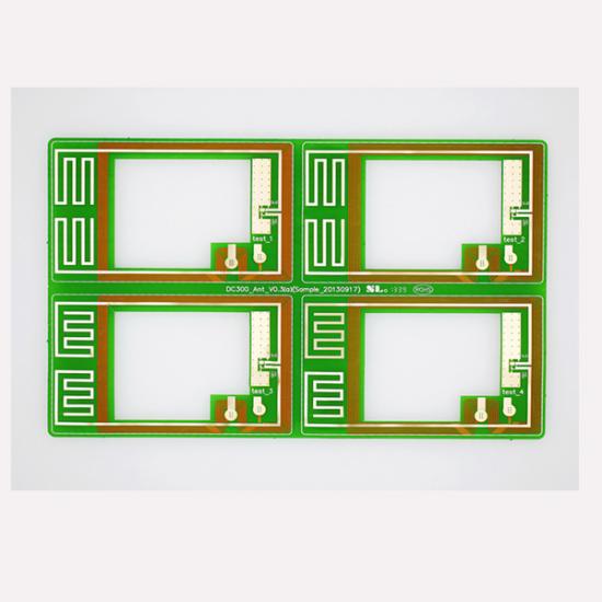
Understanding the Manufacturing Process of Flexible PCBs
The Essence of Flexible PCBs

Flexible printed circuits (FPCs) are a revolutionary technology that has transformed numerous industries, from consumer electronics to medical devices. They offer unparalleled flexibility, miniaturization, and performance, making them an ideal choice for a range of applications.
The Beginnings of Flexible PCBs
The manufacturing process of flexible PCBs starts with the design phase, where engineers lay out the circuit using software. The design must take into account the desired flexibility, component placement, and any folding requirements.
Fabrication: Layers upon Layers
The next step involves the lamination of several thin layers of copper onto a flexible substrate, such as polyimide or Kapton. This lamination process ensures that the copper layers remain attached to the substrate.
Patterning: Shaping the Circuit
After lamination, the substrate is sent through a patterning process where the desired circuit design is etched into the copper layers. This step utilizes photolithography, a technique that removes the unwanted copper while leaving the circuit pattern intact.
Component Attachment and Testing
In the next phase, surface-mounted components are attached to the circuit using precision placement equipment. Following component attachment, the flexible PCB undergoes rigorous testing to ensure functionality and reliability.
Final Assembly and Delivery
Finally, the completed flexible PCBs are inspected, packed, and delivered to customers. The entire manufacturing process is highly complex and requires meticulous attention to detail.
Conclusion
Understanding the manufacturing process of flexible PCBs is crucial for anyone working with this technology. It involves several intricate steps that require precise engineering and technological expertise. With this knowledge, engineers can optimize designs, improve manufacturing efficiency, and ultimately create better performing flexible PCBs for a range of applications.


