
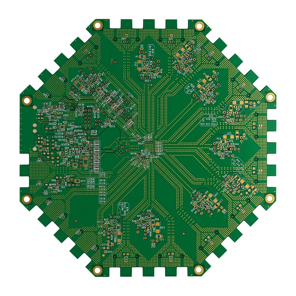
The Manufacturing Process of High-Quality FR-4 PCBs
Printed circuit boards (PCBs) are integral to modern electronics, serving as the foundation upon which most electronic devices operate. Among the various types of PCBs, those made with FR-4 material are particularly popular due to their excellent mechanical and electrical properties. In this article, we will delve into the manufacturing process of high-quality FR-4 PCBs, highlighting the critical steps involved in ensuring their superior performance.
What is FR-4?
FR-4 is a grade designation for flame-resistant fiberglass-reinforced epoxy laminate material. It is widely used in the PCB industry due to its good strength-to-weight ratio, low water absorption, and excellent electrical insulating properties. The "FR" stands for "flame retardant," indicating its ability to withstand high temperatures without burning.
Step-by-Step Manufacturing Process
Material Preparation
The process begins with preparing the FR-4 laminate, which consists of woven fiberglass cloth impregnated with epoxy resin. These laminates are pre-treated to ensure they are free from contaminants and ready for further processing.
Design Transfer
The PCB design, typically created using CAD software, is transferred onto the FR-4 laminate. This involves printing the design onto a photoresist film, which is then placed on the laminate. The film is exposed to UV light, hardening the photoresist in areas that form the circuit pattern.
Etching
After exposure, the unexposed photoresist is washed away, revealing the copper beneath. The board is then subjected to an etching process, typically using a chemical solution that removes the unwanted copper, leaving only the desired circuit pattern intact.
Drilling
Precision drilling machines create holes in the PCB for components and interconnections. These holes must be accurately positioned and sized according to the design specifications.
Plating
The next step involves plating the drilled holes and the surface of the PCB with a thin layer of copper. This enhances electrical connectivity and prepares the board for subsequent soldering of components.
Solder Mask Application
A solder mask is applied to the PCB to insulate and protect the copper traces from oxidation and to prevent solder bridges during component soldering. The solder mask is typically a green epoxy that is applied and then cured under UV light.
Silkscreen Printing
Important information such as component labels, logos, and part numbers are printed onto the PCB using a silkscreen process. This step ensures that assembly and troubleshooting are more straightforward.
Surface Finishing
The PCB surface is finished to improve solderability and protect against corrosion. Common finishes include HASL (Hot Air Solder Leveling), ENIG (Electroless Nickel Immersion Gold), and OSP (Organic Solderability Preservatives).
Inspection and Testing
High-quality FR-4 PCBs undergo rigorous inspection and testing to ensure they meet the required specifications. This includes visual inspections, electrical tests, and functional tests to verify the integrity and performance of the circuits.
Cutting and Packaging
Finally, the PCBs are cut into individual units, cleaned, and packaged for shipment. Proper packaging ensures that the boards are protected from physical damage and contamination during transportation.
Conclusion
The manufacturing process of high-quality fr-4 pcbs is complex and involves several critical steps to ensure the final product meets stringent performance standards. By understanding each phase of this process, manufacturers can produce reliable and efficient PCBs that form the backbone of countless electronic devices. Whether for consumer electronics, industrial machinery, or advanced communication systems, FR-4 PCBs continue to be a vital component in modern technology.


