
The Essential Guide to Designing Rigid PCBs for Electronic Devices
Designing rigid PCBs (Printed Circuit Boards) is a crucial step in the development of electronic devices. Whether you're a seasoned engineer or a novice designer, understanding the fundamentals of PCB design is essential for creating reliable and efficient electronic products. In this comprehensive guide, we'll walk you through the essential principles, considerations, and best practices for designing rigid PCBs for electronic devices.
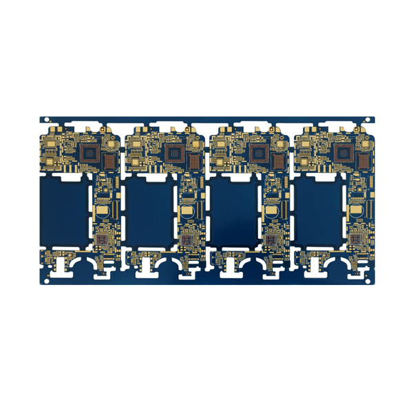
Understanding Rigid PCB Basics:
Begin by familiarizing yourself with the basics of rigid PCBs. Learn about the different layers, components, and materials that make up a typical PCB. Understand the role of copper traces, vias, pads, and solder masks in the functionality and reliability of the board.
PCB Design Software and Tools:
Choose the right PCB design software and tools for your project. Explore popular options such as Altium Designer, Eagle, KiCad, and OrCAD. Learn how to use these tools to create schematic diagrams, layout PCBs, and perform simulations to ensure optimal performance.
Schematic Design:
Start the design process by creating a schematic diagram of your electronic circuit. Clearly define the components, connections, and signal paths. Organize the schematic in a logical and intuitive manner to facilitate easy understanding and troubleshooting.
PCB Layout Design:
Once the schematic is complete, transition to the PCB layout design phase. Place components strategically on the board to minimize signal interference, optimize routing, and ensure efficient thermal management. Pay attention to factors such as component spacing, trace widths, and via placement to meet design specifications and manufacturing requirements.
Signal Integrity and EMC Considerations:
Ensure proper signal integrity and electromagnetic compatibility (EMC) by following best practices in PCB layout design. Minimize signal distortion, crosstalk, and electromagnetic interference (EMI) through careful routing, grounding, and shielding techniques. Perform simulations and analysis to validate the design and mitigate potential issues.
Design for Manufacturability (DFM) and Assembly (DFA):
Design your PCB with manufacturability and assembly in mind. Consider factors such as panelization, solder mask alignment, and component orientation to streamline the manufacturing process and minimize costs. Optimize the design for automated assembly techniques such as surface mount technology (SMT) and through-hole assembly.
Thermal Management:
Address thermal management challenges in your PCB design to prevent overheating and ensure long-term reliability. Incorporate heat sinks, thermal vias, and proper component placement to dissipate heat effectively. Consider environmental factors and operating conditions to design PCBs capable of withstanding temperature variations and thermal stress.
Design Verification and Testing:
Before finalizing your PCB design, perform comprehensive verification and testing to validate functionality, performance, and reliability. Use simulation tools, prototyping, and testing methodologies to identify and resolve any design flaws or issues. Conduct rigorous testing to ensure compliance with industry standards and regulatory requirements.
Conclusion:
Designing rigid PCBs for electronic devices requires a combination of technical expertise, creativity, and attention to detail. By following the essential principles, considerations, and best practices outlined in this guide, you can create reliable, efficient, and high-quality PCB designs that meet the needs of your electronic projects.
Send PCB Files to Sales@ucreatepcba.com, We Will Quote You Very Soon!
Request PCB Manufacturing & Assemble Quote Now


