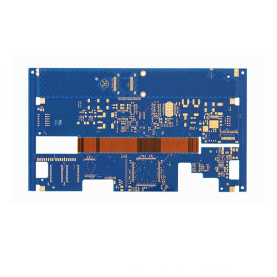
How to Judge PCB Surface Process by Color?
PCB (Printed Circuit Board) is one of the indispensable components in electronic equipment. Surface treatment is a very important step in the PCB manufacturing process as it can affect the performance and durability of the PCB. Usually, the state of PCB surface treatment can be judged by color. Next, this article will introduce in detail how to judge the surface treatment process of PCB by color. First of all, for the non-pad surface treatment of PCB, we can use color as the basis for judgment. The base material of the PCB is usually yellow or light green, and the color of the non-pad surface treatment will be different from this basic color. Common padless surface treatments include OSP (Organic Solderability Preservatives) treatment and ENIG (Electroless Nickel Immersion Gold) treatment.
As an alternative to lead-free soldering, OSP prevents oxidation of the copper surface while providing good solderability. The color of OSP is usually dark green or dark orange. This is because during the OSP process, substances are adsorbed on the surface of the substrate to form a thin film. The color of this film depends on the type and thickness of the adsorbate.ENIG is a high-end surface treatment technology that is widely used in high-precision electronic products. ENIG uses a layer of nickel and a layer of gold on top of the underlayment. Typically, the color of the underlayment in this treatment is light yellow or gold. If used incorrectly or treated for too long, the color on the metal layer will turn gray.For the pad treatment on the surface of the PCB, its surface treatment quality can also be judged by its color. Common surface treatment processes include HASL (Hot Air Solder Leveling) treatment, lead-tin alloy treatment, OSP treatment, etc.
HASL treatment is a widely used surface treatment technology. In this process, the PCB coated with solder paste passes through the melting tank, so that the tin on the solder paste is evenly combined with the solder pads on the surface of the copper board. During HASL treatment, a black or silver-gray solder layer will appear on the surface. This is because the heating process will cause oxidation or chemical reactions of the metal elements in the solder paste, making the outer color of the solder layer different from that of the PCB matrix.
Pewter treatment is another commonly used surface treatment technique. In this process, the PCB coated with solder paste is subjected to high temperature and soaking, so that the metal elements on the coating react chemically with the surface of the substrate to form a firm solder joint. During the pewter treatment, the surface takes on a bright silver or dark gray color. It depends on the time and temperature of the treatment, the longer the treatment time, the darker the color.
Finally, OSP treatment can also be used for the surface treatment of PCBs with pads. OSP can also be used for surface treatment of PBC with Through-hole, but currently it is mainly used for SMT (Surface Mount Technology) type PCB surface treatment. When OSP is processed, it is similar in color to padless processing, usually dark green or dark orange.

Send PCB Files to Sales@ucreatepcba.com, We Will Quote You Very Soon!
Request PCB Manufacturing & Assemble Quote Now


